First published in Converting Quarterly, Quarter 4: 2015 issue.
Written by Harper GraphicSolutions West Coast technical graphics advisor, Trevor Schroeder
Introduction
One of the core promises of the developing printed-electronics market is the ability to manufacture flexible-electronics products using traditional roll-to-roll (R2R) printing processes at higher speed, ultimately creating a high-value item at a low per-item cost. Many firms and universities involved in printed electronics research are focused on improving the advanced materials for this type of application. Current research is heavily focused on ink and coating formulations, especially low-cost conductive inks (the Holy Grail of printed electronics) and substrates that are printable and do not distort during the high temperature or energy required to cure the ink.
Background
Initial expectations of printed microchips have been set back several years by a number of practical challenges that warrant further research. Lowering costs of traditional microchip fabrication has spurred printed-electronics researchers to pursue a more pragmatic direction. Conductive pathways and their applications (antennae, basic circuits, sensors, etc.) have emerged with modern capabilities of print manufacturing. Today, there is significant improvement in the quality of conductive inks, resulting in improved printability and better reliability. Advancements in curing and annealing technologies have significantly improved the capabilities of wide scale manufacture. While the direction of printed electronics is still being determined, there will undoubtedly be many creative applications made possible from the rapidly evolving industry.

FIGURE 1. A flexible, touch keyboard sensor with conductive grid printed on film; the fine grid lines are designed to remain as transparent as possible while meeting the electrical requirements of each key sensor.
Printed electronics is best grouped under the umbrella term “functional printing.” This can be roughly defined by printing that serves a purpose other than graphic, visual appeal. To be considered functional printing, an object serves a function based on science (physics and chemistry), which can be one of many forms, including 3D objects printed with electrical circuits, chemical compounds, conductive pathways or pharmaceutical applications. Each printed item serves to assist, aid or otherwise interact with a user or device; for example, RFID antennae aid transmission of information between chip and reader. While currently used for inventory control and keycard access, the future of radio transmission devices may include hybrid devices that merge electronics with flexible pathways (i.e.: wearable electronics). A functional item also may be a sensor that alerts when the threshold of a specific chemical is present, such as fruit ripeness in food packaging. Functionally printed items may be concealed or visible. Conductive touch-sensor layers may be designed to remain transparent, while backing layers may wish to mask and conceal (see Figure 1).
Print-manufacturing capabilities
The construction of conductive pathways has evolved from wires to chemical and now to laser etching over years of improvements. Exploring non-screen printing processes is a more recent method that leverages technological advancement from centuries of graphic print manufacturing. Today’s presses and equipment have tight registration, refined impression control, high speed and unparalleled productivity. By replacing the graphic ink with conductive ink, electronic pathways can be printed at high speeds on a wide variety of substrates. High speed for printed-electronic applications currently ranges from 100 to 300 fpm, representing a 10- to 50-fold increase over traditional manufacturing methods. High speeds for graphic applications have reached up to 2,000 fpm because of improvements in every component in the process. It is not unreasonable to foresee an increase in speed for printed electronics applications in the future.
Conductive-ink technologies
Conductive inks can be manufactured out of metallic components (i.e.: flake silver, nanosilver, copper) or carbon-based (i.e.: graphene) and are very expensive because of the required conductive components when compared to pigment-based inks. One fundamental conductive pathway, a trace line, connects two nodes on a circuit. Usually trace lines are designed as thin as possible to control costs, minimizing the amount of expensive conductive ink required to complete the circuit. The carriers of the conductive particles are primarily water- and solvent-based ink components.
After printing, the water or solvent is evaporated, and the conductive particles and any necessary binding agents are left in direct contact with each other and the substrate. These dried particles typically require curing before they exhibit their conductive or insulating nature. Curing may be completed by means of sintering and/or heat curing to coalesce or fuse particles into an uninterrupted conductive pathway. Substrates must withstand sintering or heat curing without deformation or degradation.
Printing methods
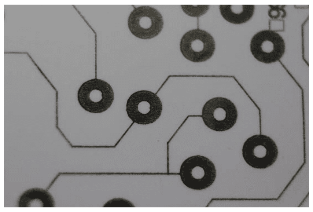
FIGURE 2. Conductive trace lines with node attachment points; trace lines may be printed in any direction but should be tested for differences in printability in both the machine- and cross-directions.
Conductive inks are being printed on substrates using many processes, including gravure, flexography, screen printing, inkjet, offset lithography, slot-die coating and blade coating, among others. Each process has advantages, limitations and requirements – each requiring specific ink/coating rheology for optimum performance. Each printing process has limitations on print features that impact conductivity, with trace line width, ink film thickness and ink film evenness being the most critical (see Figure 2).
For example, screen printing can deposit a very thick film of ink compared to other processes but may not be able to deposit as fine a trace line as flexography. These tradeoffs are common not only between print processes but also within each printing process itself. Fluid dynamics and mechanical attributes of each printing process need to be considered: Trace lines may print better in the machine direction (in line with a web or sheet) when compared to the cross-direction in R2R applications.
Due to the variety of packaging processes and their associated tradeoffs, the following is a quick review of each print process and its capabilities and limitations.
Flexography: Flexography uses a raised-image printing plate created in a relief platemaking process. Plate materials are either photopolymer or rubber and can be easily changed for a variety of artwork or circuit-design applications. The printing plate transfers a film of ink to the substrate after contacting a metered ink film on the anilox roll. The anilox engraving can be changed to vary the ink film thickness. Flexography has two ink splits (plate/anilox and plate/substrate) and delivers a 19-23% deposition. The flexographic process has printed trace lines as thin as 15-30 microns while ink film thicknesses typically range from 0.20-4.0 microns. Ink is fluid at approximately 100-1000 centipoise (cPs).
Gravure: Also known as rotogravure, gravure is a relief process that uses an imaged cylinder with recessed cells to deposit ink onto a substrate. The ink film is controlled by the size and pattern of the engraved cells, which are metered by a doctor blade leaving ink in the recessed print areas while unengraved areas (non-print areas) are wiped clean. Because the metered ink film from the gravure cylinder directly contacts the substrate, it only has one ink split and deposits 40-44% of the ink from the cells to the substrate. Ink film thickness ranges between 0.40-6.0 microns, and minimum engraved trace line width ranges between 5-40 microns, although trace lines narrower than 25 microns present a challenge. Gravure requires fluid ink between 50-750 cPs. Offset gravure adds a transfer blanket roll to the gravure process making it similar to flexography (two ink splits); however, the distinction is that the image is still created with the engraved gravure roll. The transfer roll only exists to transfer the ink from the imaged areas to the substrate. This is useful for rigid, rough, textured and shaped substrates that otherwise would not fully contact a hard gravure cylinder.
Screen printing: Screen printing is the forcing of ink through a mesh screen. The mesh is masked in non-printing areas and does not allow ink to flow through. Screen printing, by its nature, is able to deposit a thick layer of ink ranging from 1-200 microns. Because there is a large amount of ink deposited, trace lines tend to be much larger at 50 microns, while ink viscosities can be much thicker up to 70,000 cPs.
Inkjet: Inkjet uses a small nozzle to eject very fluid ink and deposit small droplets onto a substrate. Particles must be very small to pass through the inkjet nozzle with nano inks being most common. Trace lines and minimum print features are dependent on droplet size, but can range from 3-20 microns while the ink film thickness is determined by droplet size and number of passes. When compared to the aforementioned processes, inkjet is computer-intensive as each droplet is calculated and plotted. The necessary processing horsepower has traditionally limited the speed of the printing process.
Considerations for printed-electronic design
When starting with an idea of an end product, it is important to determine the necessary process best suited for the application. Ink film thickness and minimum print features will directly impact conductivity and other properties required for circuitry (how many pathways can fit in a two-dimensional area). Press speed and production needs must be considered as each process is capable of a certain throughput capacity; R2R processes typically outpacing other methods.
Clearly, there are a variety of methodologies to construct an electronic pathway with a high number of input variables to consider. While most designs start with a vision of an end product, the research required to construct that product is extensive. For companies manufacturing specific sub-components using functional inks and substrates, the testing of all materials is the key to a successful product development process.
Testing methodologies
Four different levels of testing exist, each with their own benefits and barriers: outsourcing, small-scale laboratory testing, medium scale pilot testing and finally, full-scale production testing.
Outsourcing is an option for processes that are easily defined and can be tested with established, controlled parameters. These parameters need to be thoroughly communicated between development engineers and laboratory technicians performing the test. As the printed-electronics market is emerging, outsourcing is a limited option at present.
The testing of all materials is the key to a successful product development process.
Small-scale laboratory testing can be completed with limited capital investment and provides the ability to test inks while determining important parameters that affect printability: viscosity, solids content, drying, rewetting and ink-substrate compatibility. Small-scale testing allows conductivity to be measured and ink performance to be evaluated. Trace line widths and ink film thickness can be tested and adjusted as necessary. Ideally, this laboratory testing can be completed with very little consumption of high-cost inks and substrates.
Medium-scale pilot testing can be completed with custombuilt equipment or selected components from widely available converting equipment. This stage is intended for small print runs that prove the concept for full-scale testing.

FIGURE 3. Proprietary proofing system with flexo-plate cylinder and mounted EPDM plate for conductive-ink testing
Full-scale production testing is a final step in the development cycle and most likely would require a partnership between a laboratory and converter. This final step incorporates the experience and expertise of the converter with the engineering requirements of the developer using the inks and substrates that have been previously validated on smaller scale equipment.
Multi-process system for laboratory testing
One solution offered by this firm is targeted directly at both laboratory-scale and potential production testing. A new proprietary proofing system was originally developed for flexographic and gravure ink mixing and color matching. In 2010, Harper was approached by a university looking to test flexography and gravure on a small laboratory scale for printed electronics research and provide demonstrations of their research at the FlexTech Alliance tradeshow, 2015FLEX. The design of the system was readily expanded to become a multi-process platform.
Today, the proprietary proofing system can replicate flexography flood coating, flexography with imaged plates, direct gravure and offset gravure. The system uses a flatbed printing platform and is capable of depositing inks between 2.75-5.0 in. wide and up to 27 in. in print length. A small amount of ink is placed between the doctor blade and the anilox or gravure cylinder on the appropriate printhead; the printhead then traverses a stationary substrate that can range from thin films to 3/16-in. rigid glass or board. After the drawdown, the printhead is removed without tools for quick and easy cleaning. Using pipette-applied ink reduces the amount of expensive inks since there is no need to fill a pan or chamber. Each drawdown can be evaluated for printed properties, and subsequent trials can be adjusted as necessary.
The proofer table is available in manual, electric or pneumatic power, allowing the researcher to select a model that prints at the required speed. During initial testing, it was found that consistent loading pressure is a crucial parameter. Impression is controlled by a spring-loaded lever arm that holds the printhead against the substrate. Springs are changeable to find the correct loading pressure for the image, ink and substrate.
For flexographic models, printheads are available with repeat sizes of 2.356 in. and 6.67 in. to test a variety of applications. Plateheads are available as in-the-round engraved EPDM rubber or a plate cylinder for mounting photopolymer or EPDM plates in 0.067-in. and 0.045-in. thicknesses (see Figure 3). Anilox rolls are easily changed to alter ink deposition and test a variety of ink film thicknesses.
Ink film thickness of a particular ink is a direct variable in the conductivity of a pathway.
For projects with circuitry design, a photopolymer plate can be changed easily and is durable enough to be mounted and unmounted many times. It has been found that the new proofing system is very useful for testing a variety of plate materials and the latest plate-manufacturing technologies. Flat-top dots, platesurface texturing and dual-durometer plates can be tested to see how they interact with different inks and substrates. Testing imaged patterns or flood coats can be used for ink development to see how inks lay down with different conductive particle sizes and resin systems. Using the modular nature and its flexibility, the proofer can be used for multilayers and even multiple processes by adding registration marks to the imaged materials. With sufficient trap (overlap) between layers, even complex projects can be tested.

FIGURE 4. Proprietary proofer with direct gravure XDI cylinder printing conductive-ink test patterns on film. (Courtesy of Tony Donato, product development engineer, Harper Corp. of America)
Ink film thickness of a particular ink is a direct variable in the conductivity of a pathway. In graphic printing, the ink film thickness directly relates to the visual strength associated with a particular ink film; certain pigments require certain thicknesses of ink to achieve a desired color. Anilox rolls deliver ink to the printing plate and various thicknesses can be achieved by changing the linescreen, volume or geometry of the engraving. The amount of ink delivered can be tested to determine the conductive or resistive nature of the ink. The new proofing system uses this firm’s laser-engraved ceramic cylinders as flexographic anilox rolls or gravure imaged engravings (see Figure 4). Harper has the ability to laser-engrave ceramic cells as fine as 2,000 cpi with 0.5 bcm to 70 cpi with 40.0 bcm for the new proofer (cpi = cells per inch; bcm = billion cubic microns per sq inch of engraved surface area).
Both flexography and gravure printing use engraved cells for ink deposition, and therefore print quality is directly dependent on engraving linescreen, volume, and geometry. The new proofer can use engravings, such as traditional 45º quad, 60º hexagons, elongated hexagons, channels and open-cell structures. The different engraving geometries may affect the performance of the ink, and thus, small, changeable rolls benefit the research process.
Other attributes of printability can be tested through iterations of drawdowns, such as ink drying and curing, which are both important factors in successful printing: 1) If an ink easily rewets due to high resolvability before curing, applying multiple passes may pose a challenge; 2) If an ink does not easily rewet, ink can dry onto the plate, anilox or gravure roll, proving difficult to keep the small cells open. Cleaning methods can be evaluated for effectiveness and resin systems can be adjusted for improved printability. Understanding how an entire process will scale to full production improves development time and saves valuable press time in the future.
Conclusion
For many engineers considering high-output applications, flexography and gravure are promising for their high-speed, R2R applications on a variety of substrates. Establishing a project outline is critical especially when developing printed electronics and other functional projects. Work with material suppliers and equipment suppliers to understand necessary starting materials. Leaning on the expertise of suppliers for technical assistance can save valuable research time and help avoid common pitfalls.
What can be learned from using this firm’s new proprietary proofing system to test conductive inks is up to your imagination. We want you to excel in developing your new product for this exciting, emerging industry.
 About the Author: Trevor Schroeder, West Coast technical graphics advisor for Harper GraphicSolutions, a division of Harper Corp. of America (Charlotte, NC), holds a bachelor of science degree in graphic communication from Cal Poly (San Luis Obispo, CA) and a master’s of science in print media from the Rochester Institute of Technology. His past work has focused on adopting new technologies in conventional printing and converting businesses, and he currently supports the HarperScientific QD and the universities and researchers testing conductive materials on the system.
To view the original Converting Quarterly article click HERE.


